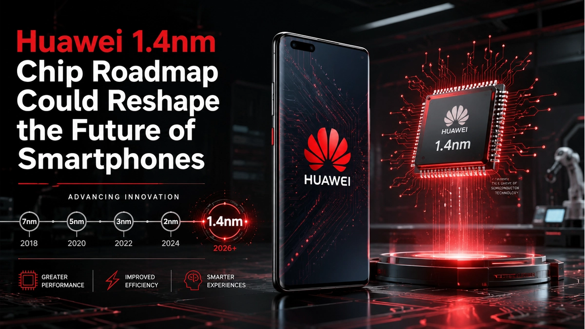
Huawei 1.4nm Chip Roadmap Could Reshape the Future of Smartphones
 By Inflix
 Huawei has made a bold claim in the semiconductor world. The company says it wants to reach 1.4nm-equivalent chip density by 2031 through a new semiconductor development framework called Tau Scaling Law. In simple words, Huawei is trying to find a new way to make powerful chips without fully depending on the most advanced chipmaking machines used by companies like TSMC, Intel and Samsung.
This is important because Huawei has been under major US restrictions for years. These restrictions have limited its access to advanced semiconductor tools. However, instead of only waiting for access to next-generation machines, Huawei appears to be working on a different route. Its new approach focuses on better chip architecture, shorter signal paths and improved transistor density.
For smartphone users, this could become a major story over the next few years. If Huawei succeeds, future phones could become faster, more efficient and better at handling AI features. However, there is still one important point to understand: Huawei is talking about 1.4nm-equivalent transistor density, not necessarily traditional 1.4nm manufacturing in the same way TSMC or Samsung describe their future nodes.
What Are Huawei 1.4nm Chips?
Huawei 1.4nm chips refer to the company’s long-term target of creating high-end chips with transistor density similar to what the industry expects from a 1.4nm process. According to reports, Huawei expects to reach this level by 2031 through its new semiconductor framework.
Usually, chipmakers improve performance by shrinking transistors. Smaller transistors can help chips become faster, more power-efficient and more suitable for advanced phones, laptops, AI servers and data centres. However, shrinking chips is becoming harder and more expensive. Therefore, companies are now looking at new methods, including advanced packaging, 3D stacking and architecture-level improvements.
Huawei’s plan seems to follow that direction. Instead of only chasing smaller physical nodes, the company is trying to improve how signals move inside the chip. As a result, it hopes to increase real-world performance and density without depending fully on extreme ultraviolet lithography machines.
What Is Tau Scaling Law?
Huawei’s new Tau Scaling Law is being presented as an alternative way to keep improving chip performance in the post-Moore’s Law era. Moore’s Law traditionally suggested that the number of transistors on a chip would continue to grow rapidly over time. However, the industry has slowed down because advanced chip production is now extremely complex and costly.
Tau Scaling Law focuses on improving how efficiently a chip works internally. Instead of only reducing transistor size, the idea is to reduce signal delay and improve density through new architecture. Huawei has also connected this strategy with a technology called LogicFolding, which is designed to reduce resistive and capacitive load during signal propagation.
In easier words, Huawei wants to make chips smarter from the inside. If data can move faster and more efficiently across the chip, the processor may deliver better performance even if the manufacturing tools are not as advanced as those used by global leaders.
Why LogicFolding Matters
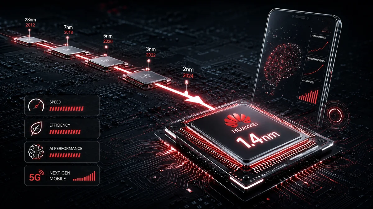
LogicFolding is one of the most interesting parts of Huawei’s semiconductor plan. According to available reports, this architecture aims to improve chip density by changing how circuit layers and signal paths are arranged. It may help Huawei reduce the distance signals need to travel inside the chip.
This matters because modern chips are not only limited by transistor size. They are also limited by heat, power usage and signal delay. Therefore, a better internal layout can improve performance even when the manufacturing node is not the most advanced.
For smartphones, this could mean better AI processing, improved battery life and faster app performance. In addition, it could help Huawei build stronger Kirin chips for future flagship phones.
Why This Is Important for Smartphones
Smartphones now depend heavily on powerful processors. Camera processing, gaming, video editing, AI assistants, live translation and on-device privacy features all need strong chips. Therefore, any major change in chip design can directly affect future smartphones.
If Huawei 1.4nm chips become a reality by 2031, they could help the company compete more strongly in flagship devices. Huawei already has a strong position in camera hardware, battery technology and software optimisation. However, advanced chips remain one of the biggest challenges because of global supply restrictions.
A successful 1.4nm-equivalent roadmap could give Huawei more control over its future phones. As a result, the company may rely less on foreign chip technology and more on its own semiconductor ecosystem.
Could Huawei Compete With TSMC and Samsung?
Huawei’s target is ambitious. TSMC, Samsung and Intel are already working on highly advanced chip nodes, and they have access to some of the most advanced semiconductor tools in the world. Huawei, on the other hand, is trying to close the gap while facing export restrictions.
That makes this roadmap both exciting and uncertain. Huawei may be able to improve performance through chip architecture, but mass production is another challenge. Making a design work in theory is not the same as producing millions of reliable chips at scale.
Experts also point out possible issues such as heat management, software complexity and manufacturing yield. Therefore, Huawei’s 2031 goal should be seen as a long-term roadmap rather than a guaranteed product launch.
Huawei’s Chip Push and US Sanctions
Huawei’s semiconductor work is also linked to the wider US-China technology rivalry. Since Huawei was added to the US trade blacklist in 2019, the company has faced serious limits on advanced chips and semiconductor tools. More restrictions followed in later years, especially around high-end chipmaking equipment and AI hardware.
Because of this, Huawei has been investing heavily in local chip development. The company’s recent progress with Kirin and Ascend chips shows that it still wants to compete in both consumer devices and AI computing. In fact, Huawei has already become one of the most important companies in China’s technology self-reliance push.
The new 1.4nm-equivalent roadmap adds another layer to that strategy. It suggests Huawei does not only want to survive restrictions. It wants to create a different path for advanced chip development.

What It Means for AI Phones
AI phones are becoming one of the biggest trends in mobile technology. Brands are adding on-device AI tools for writing, image editing, voice assistance, search, photography and privacy protection. However, these features need powerful and efficient chips.
Huawei 1.4nm chips could make future AI phones more capable. For example, a more advanced Kirin processor could run complex AI models directly on the device. This would reduce cloud dependency and improve privacy. In addition, it could make AI features faster because the phone would not always need to send data to remote servers.
However, the real impact will depend on how Huawei turns this roadmap into working products. If the company brings LogicFolding-based chips to smartphones before 2031, users may start seeing early benefits sooner.
Will Huawei 1.4nm Chips Launch in Phones by 2031?
At the moment, Huawei’s 2031 target appears to be about reaching 1.4nm-equivalent chip density. It does not mean a Huawei phone with a 1.4nm chip is confirmed for launch in 2031. The company still needs to prove that this technology can work at scale.
However, the roadmap suggests Huawei is planning for the next generation of mobile and AI processors. If development goes well, future Kirin chips could become much more competitive. Therefore, this news is important for anyone following smartphone innovation, AI phones and the future of mobile processors.
Why This Could Change the Semiconductor Race
The semiconductor industry has long depended on expensive manufacturing equipment and advanced lithography. Companies with access to these tools have a major advantage. Huawei’s approach challenges that model by suggesting architecture-level innovation could help close the gap.
If Huawei succeeds, other companies may also explore similar routes. This could make the chip industry more competitive and less dependent on one method of scaling. On the other hand, if the approach fails to scale, it may show that advanced manufacturing equipment remains essential for leading-edge chips.
Either way, Huawei’s 1.4nm roadmap is a major signal. The company is not stepping away from advanced chips. Instead, it is trying to rewrite the rules of chip development.
Should Smartphone Buyers Care Right Now?
For everyday smartphone buyers, this news will not change buying decisions immediately. Huawei 1.4nm chips are still years away. However, the roadmap matters because it shows where future smartphones may be heading.
Over the next few years, phones will need more powerful processors for AI, camera processing and gaming. Therefore, chip innovation will become even more important. If Huawei can turn its Tau Scaling Law and LogicFolding architecture into real products, future phones could become much smarter and more efficient.
For now, users should treat this as a promising long-term development. It is not a confirmed consumer product yet, but it is one of the most interesting semiconductor stories of 2026.
Final Thoughts
Huawei’s plan to reach 1.4nm-equivalent chip density by 2031 is a bold move. The company is trying to overcome major technology restrictions by creating a new scaling method instead of following the traditional path only.
The biggest takeaway is simple: Huawei wants to compete in the future of advanced chips, AI phones and high-performance computing. Its Tau Scaling Law and LogicFolding architecture could become important if they work at mass-production scale.
However, there are still many challenges ahead. Heat, yield, software complexity and large-scale manufacturing will decide whether this plan becomes a real breakthrough or remains an ambitious roadmap. Still, for the smartphone industry, this is a story worth watching closely.
FAQs About Huawei 1.4nm Chips
What are Huawei 1.4nm chips?
Huawei 1.4nm chips refer to the company’s target of reaching transistor density similar to a 1.4nm process by 2031. It is currently a long-term semiconductor roadmap, not a confirmed phone chip launch.
What is Huawei Tau Scaling Law?
Tau Scaling Law is Huawei’s new semiconductor framework. It focuses on improving chip performance and density through architecture improvements instead of only shrinking transistor size.
What is LogicFolding?
LogicFolding is Huawei’s chip architecture technology. It aims to reduce signal delay and improve transistor density by changing how logic and circuit layers are arranged.
Will Huawei launch a 1.4nm smartphone chip?
Huawei has not confirmed a consumer smartphone chip launch with 1.4nm technology yet. The current target is to reach 1.4nm-equivalent density by 2031.
Why is Huawei’s chip roadmap important?
It is important because Huawei is trying to develop advanced chips despite US restrictions. If successful, it could strengthen future Huawei phones, AI chips and China’s semiconductor industry.
For more mobile technology updates, you can also read our latest coverage on AI phones in 2026 and future smartphone trends. These guides explain how AI chips, mobile processors and software improvements may change the next generation of smartphones.
If you are planning to upgrade your phone, you can also explore trusted refurbished mobile options from Zextons Tech Store. Choosing a reliable refurbished smartphone can be a smart way to save money while still getting strong performance, better cameras and modern features.